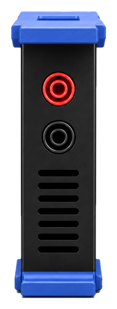
Power Supply
MB-PS240
Instrument module · MB-LA16
16 digital inputs, eight pattern outputs and a dedicated external trigger. Grouped logic thresholds, USB 3 and Gigabit Ethernet in the 2U module format.
SKU MB-LA16
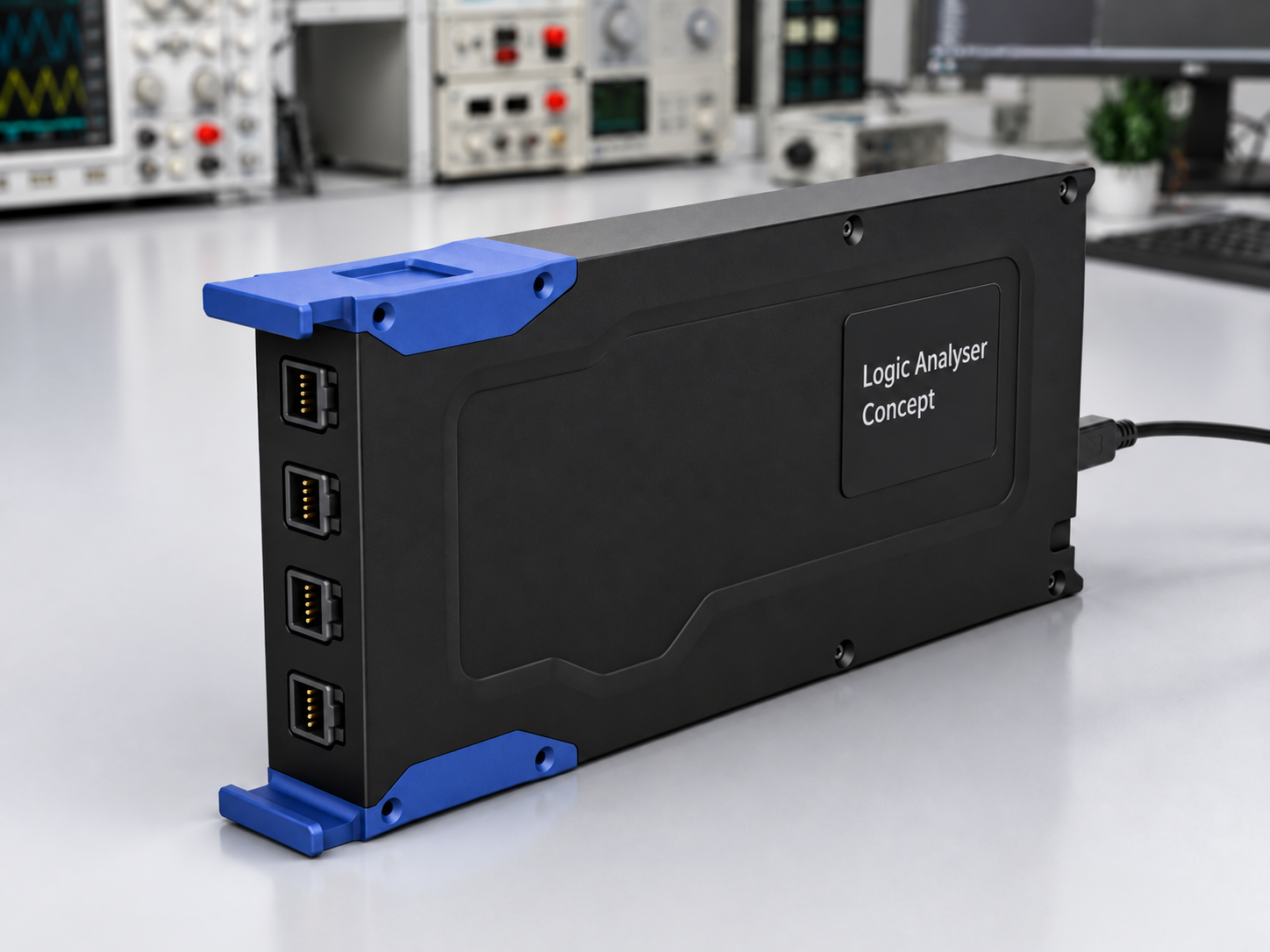
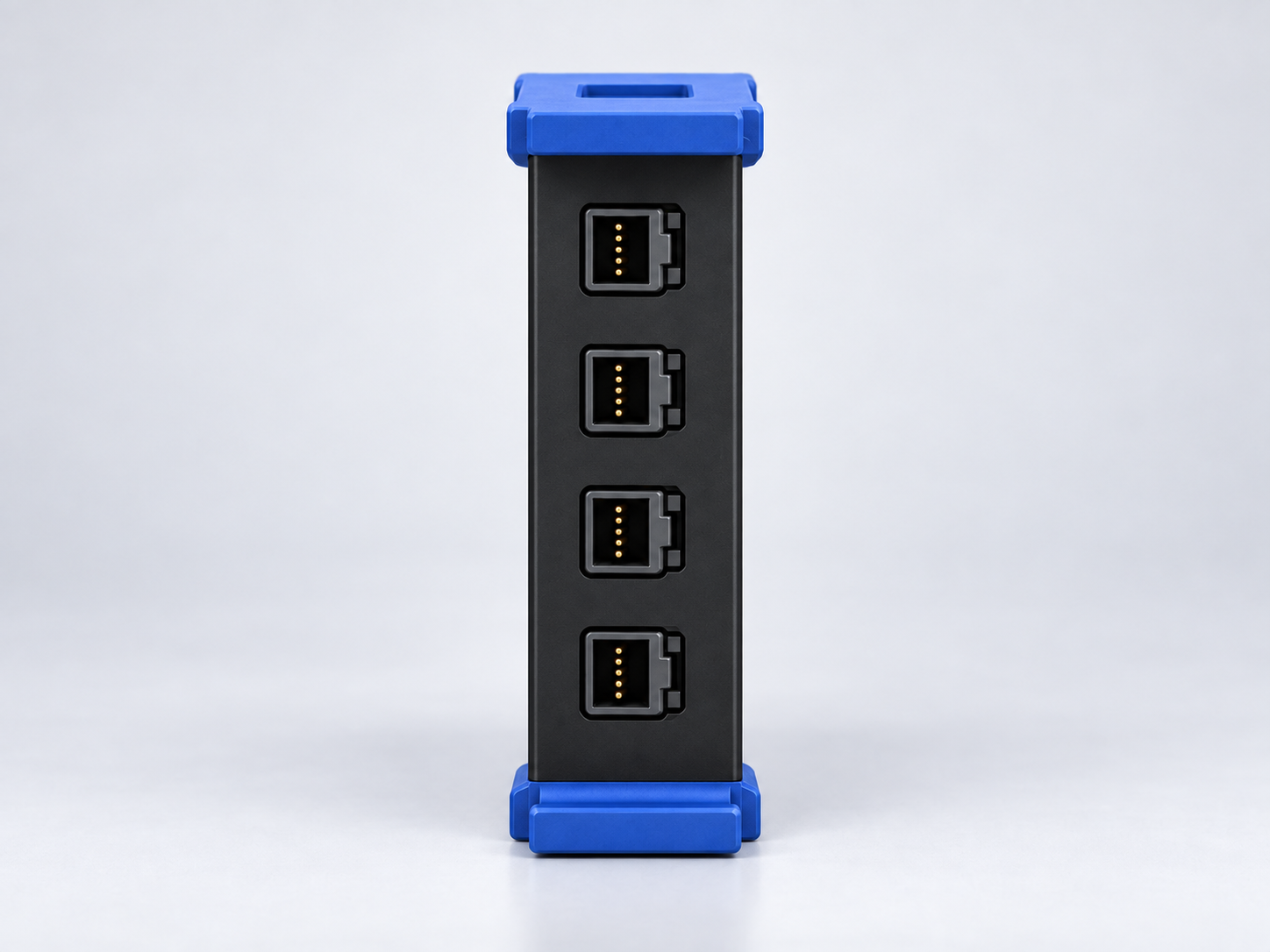
1 / 2Bench view
Software · Firmware · Gateware
The LA evaluates signal and protocol triggers in the FPGA. Control Hub combines capture analysis, decoded messages and timing measurements.
View trigger typesEdges, pulse widths, timing conditions and protocol events.
02 / DECODEI²C, SPI, UART, CAN, USB PD and more.
03 / GENERATEEight LA outputs, 34 digital recipes and a timing editor.
SOFTWARE ACCESSAll software features are included across devices.
Block diagram
Sixteen digital inputs and eight pattern outputs share one FPGA acquisition engine with DDR sample memory. The trigger input/output connects to the FPGA separately from the MCU host interfaces. Trigger input does not consume a capture channel. The MCU presents the module over USB-C 3.0 and gigabit Ethernet.
BLOCK-LEVEL · NOT A SCHEMATIC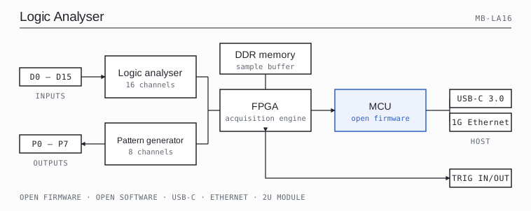
Input ranges, acquisition modes and operating conditions.
16 capture inputs with an independent threshold setting for each group of four.
| Parameter | Specification | Conditions |
|---|---|---|
| Input channels | 16 | Hardware definition |
| Threshold groups | 4 × 4 channels: 0–3, 4–7, 8–11, 12–15 | Independent group settings |
| Normal input range | 0–5 V logic | Connector voltage relative to ground |
| Logic families | 1.2 / 1.8 / 2.5 / 3.3 V CMOS; 5 V TTL and CMOS | Six defined threshold modes |
| Input frontend frequency | 200 MHz | Input frontend; sample rate is separate |
| DC input resistance | 22.68 kΩ nominal | 12.68 kΩ / 10.0 kΩ divider |
| Input current at 5 V | Approximately 220 µA | Calculated DC loading before leakage |
| Threshold calibration | Slope and offset per four-channel group | Per-group calibration |
Eight dedicated outputs, separate from the capture inputs. Each four-channel group has its own drive-voltage setting.
| Parameter | Specification | Conditions |
|---|---|---|
| Output channels | 8 | Two groups of four |
| Adjustable logic level | 1.65–3.3 V per group | Independent voltage setting for each bank |
| Nominal 5 V mode | USB-derived 5 V / 5 V CMOS | Follows source, cable and load; not precision regulated |
| Output frequency | 50 MHz | Pattern output frequency |
| Series resistance | 100 Ω per channel branch | Does not include driver or switch resistance |
| Startup state | Outputs disabled; signal paths disconnected | Hardware pull-ups; enable after rail settling |
| External drive on outputs | No sustained overvoltage rating | Outputs are not general-purpose protected inputs |
| Pattern vector clock | 100 MHz / N; 10 ns steps | Driver reports the achieved rate |
| Patterns page buffer | 4,096 vectors | Loop or one-shot; longer recipes may use a slower clock |
| Long-pattern memory | Up to 268 million vectors, memory-split dependent | Driver/API; shared memory allocation |
A dedicated trigger input/output connected to the FPGA. Trigger input does not consume a capture channel. The input specifications below do not describe output drive capability.
| Parameter | Specification | Conditions |
|---|---|---|
| Trigger interface | MCX trigger input / output | FPGA-connected interface |
| Connector / termination | 50 Ω MCX connector; high-impedance input | No 50 Ω termination fitted |
| Input resistance | 22.68 kΩ nominal | Same divider architecture as the capture inputs |
| Normal input range | 0–5 V logic | Center contact relative to MCX shell |
| Threshold setting | Independent; same six input modes | Separate trigger calibration |
| Edge selection | Rising, falling or either edge | Gateware-defined selection |
| Minimum high / low pulse | 10 ns | At the connector |
| Repetitive event rate | 50 MHz |
FPGA acquisition with DDR3L sample memory and USB or Ethernet transfer.
| Parameter | Specification | Conditions |
|---|---|---|
| FPGA | Lattice ECP5 LFE5U-45F-7BG256C | Hardware selection |
| Controller | WCH CH32H417QEU6 | USB, Ethernet and FPGA configuration controller |
| External memory | 8 Gbit (1 GiB) DDR3L, GDP3BELM-CB | Physical memory capacity |
| Memory organization | 512M × 16; two byte lanes | 16-bit memory interface |
| Memory supply mode | DDR3 at 1.5 V | Selected operating mode |
| FPGA loading | Host-supplied gateware, loaded by the MCU over Slave SPI | Default assembly has no populated configuration flash |
USB-C carries data and power. Ethernet is a separate data interface; board power comes from USB-C.
| Parameter | Specification | Conditions |
|---|---|---|
| USB | USB 3.2 Gen 1 with USB 2.0 high-speed companion | Host data interface |
| Ethernet | Gigabit Ethernet via RTL8211F-CG | CH32H417 GMAC / RGMII interface |
| Internal MCU–FPGA data bus | 16 physical UHSIF data lines, 1.8 V | MCU is the bus master |
| Power input | USB Type-C, nominal 5 V | Sink / UFP only |
| Full-operation supply | Source must advertise 3 A at 5 V | Type-C current advertisement |
| Default / 1.5 A source | Controller enumeration only | A 5 V / 3 A source is required for full operation |
| Higher-voltage USB PD | Not supported | No contract above 5 V |
| Steady-state input current | ≤2.40 A | Maximum steady-state input current |
Host-side protocol analysis and instrument hardware triggering have separate capabilities.
| Parameter | Specification | Conditions |
|---|---|---|
| Host protocol analysis | CAN / ISO CAN FD, USART, SPI, I²C, LIN, 1-Wire, Manchester, parallel and PWM | Shared Control Hub decoding |
| Advanced protocol triggers | FPGA protocol triggers | CAN, USART, CAN FD, LIN, FlexRay, USB PD, SENT and T1S; see the Features matrix |
| Negative input fault | −12 V not rated | No ±12 V protection claim |
| Enclosure | 2U module format | Modular Bench format |
| Production test documentation | Per-device reports through the customer account | Published against the supplied equipment ID |
| Software access | All features across devices; no paid unlocks | Open-source software, firmware and gateware; licence details accompany source releases |
Connector transition bands. Capture groups and the external trigger select modes independently.
| Logic mode | Connector transition band | Nominal internal VREF |
|---|---|---|
| 1.2 V CMOS | 0.49–0.71 V | 0.315 V |
| 1.8 V CMOS | 0.79–1.01 V | 0.447 V |
| 2.5 V CMOS | 1.14–1.36 V | 0.601 V |
| 3.3 V CMOS | 1.54–1.76 V | 0.778 V |
| 5 V TTL | 1.39–1.61 V | 0.711 V |
| 5 V CMOS | 2.39–2.61 V | 1.152 V |
Hardware trigger support is specified separately from host protocol decoding and the dedicated external input.
| Parameter | Specification | Conditions |
|---|---|---|
| Signal trigger types | Edge, pulse width, timeout, Nth edge, pattern, delay, setup/hold | FPGA hardware triggers |
| Trigger holdoff | 0–24 s in the LA signal engine | See Features for timing limits |
Instrument module format.
| Parameter | Specification | Conditions |
|---|---|---|
| Module format | 2U | Modular Bench format |
| Parameter | Specification | Detail |
|---|---|---|
| Module format | 2U | Modular Bench format |
| Rack capacity | 7 module positions | Modular Bench format |
| User interface | Shared touchscreen | Modular Bench format |
| Control interfaces | USB-C / Ethernet | Modular Bench format |
| Power input | USB-C | Modular Bench format |
System interfaces, software features and equipment records.
MB-PS240
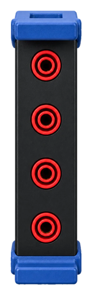
MB-DMM45
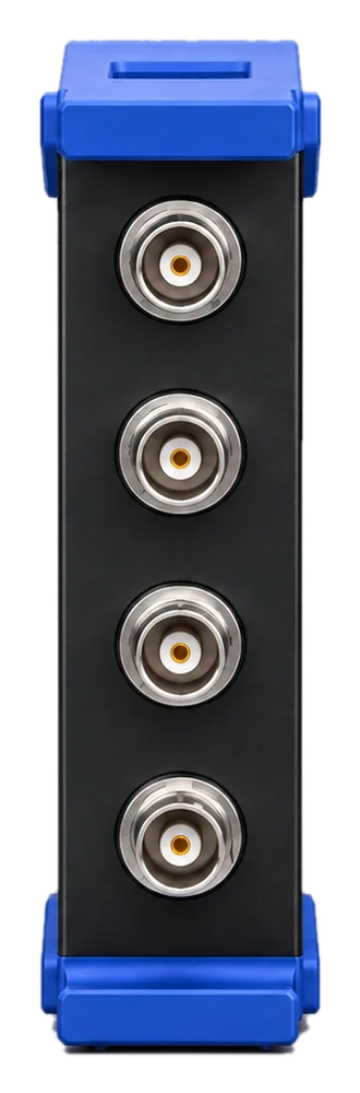
MB-SCOPE14
MB-AWG4
MB-LOAD
MB-SMU